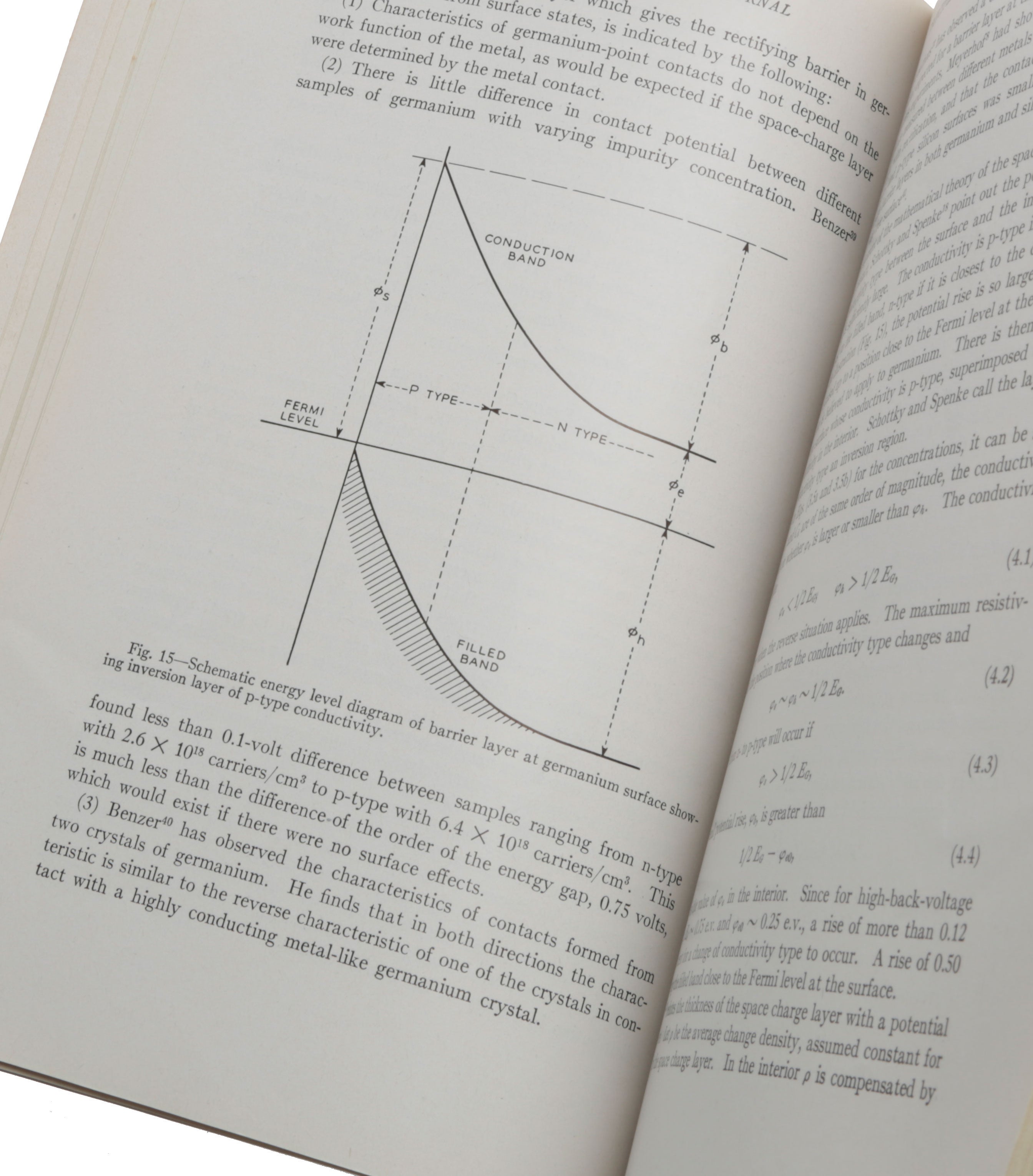


‘Physical Principles Involved in Transistor Action,’ pp. 239-77 in The Bell System Technical Journal, Vol. XXVIII, No. 2.
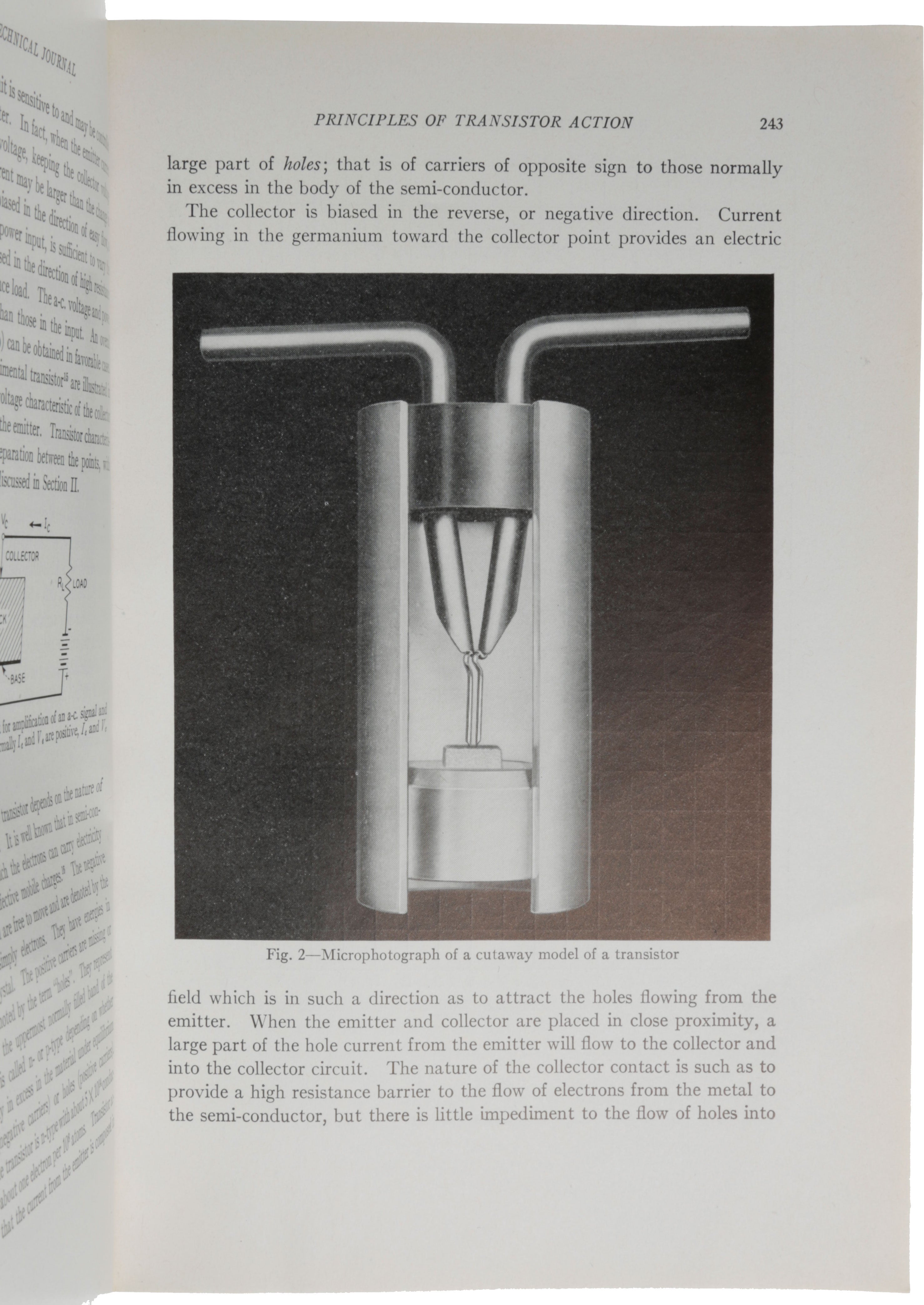
New York: American Telephone and Telegraph Company, 1949. First edition, journal issue in original printed wrappers, of the first comprehensive report on the transistor, one of the most important inventions of the 20th Century. “In the 1930s, Bell Labs scientists were trying to use ultrahigh frequency waves for telephone communications, and needed a more reliable detection method than the vacuum tube, which proved incapable of picking up rapid vibrations ... John Bardeen, Walter Brattain and William Shockley spearheaded the Bell Labs effort to develop a new means of amplification,” developing, by 1948, a novel device that would effectively amplify and control electric signals. “At roughly half an inch high, the first transistor was huge by today's standards, when 7 million transistors can fit onto a single silicon chip. But it was the very first solid state device capable of doing the amplification work of a vacuum tube, earning Bardeen, Brattain and Shockley the Nobel Prize in Physics in 1956. More significantly, it spawned an entire industry and ushered in the Information Age, revolutionizing global society” (The American Physical Society). The invention of the transistor was first announced in three short letters by Bardeen, Brattain, Shockley, and Pearson, in The Physical Review (July 1948). The following year Bardeen and Brattain published the more comprehensive report ‘Physical Principles Involved in Transistor Action’. This paper was simultaneously published, the same month, in The Physical Review and The Bell System Technical Journal. Offered here is the Bell printing [no priority established]. In 1956 Bardeen and Brattain shared the Nobel Prize in Physics with William Shockley “for their researches on semiconductors and their discovery of the transistor effect”. In 1972 Bardeen again received the Nobel Prize in Physics for his part in the development of the theory of superconductivity (BCS-theory), and thus became the only person, until this day, to receive the Nobel Prize more than once in the same field. Provenance: Regnar Holfrid Svensson (1910-90), Swedish engineer and inventor (signature to front wrapper). “The first patent for the field-effect transistor principle was filed in Canada by Austrian-Hungarian physicist Julius Edgar Lilienfeld on October 22, 1925, but Lilienfeld published no research articles about his devices, and his work was ignored by industry. In 1934 German physicist Dr. Oskar Heil patented another field-effect transistor. There is no direct evidence that these devices were built, but later work in the 1990s show that one of Lilienfeld’s designs worked as described and gave substantial gain. Legal papers from the Bell Labs patent show that William Shockley and a co-worker at Bell Labs, Gerald Pearson, had built operational versions from Lilienfeld’s patents, yet they never referenced this work in any of their later research papers or historical articles. “The Bell Labs work on the transistor emerged from war-time efforts to produce extremely pure germanium ‘crystal’ mixer diodes, used in radar units as a frequency mixer element in microwave radar receivers. UK researchers had produced models using a tungsten filament on a germanium disk, but these were difficult to manufacture and not particularly robust. Bell’s version was a single-crystal design that was both smaller and completely solid. A parallel project on germanium diodes at Purdue University succeeded in producing the good-quality germanium semiconducting crystals that were used at Bell Labs. Early tube-based circuits did not switch fast enough for this role, leading the Bell team to use solid-state diodes instead. After the war, Shockley decided to attempt the building of a triode-like semiconductor device. He secured funding and lab space, and went to work on the problem with Bardeen and Brattain. John Bardeen eventually developed a new branch of quantum mechanics known as surface physics to account for the ‘odd’ behavior they saw, and Bardeen and Walter Brattain eventually succeeded in building a working device. “The key to the development of the transistor was the further understanding of the process of the electron mobility in a semiconductor. It was realized that if there was some way to control the flow of the electrons from the emitter to the collector of this newly discovered diode (discovered 1874; patented 1906), one could build an amplifier. For instance, if one placed contacts on either side of a single type of crystal, the current would not flow through it. However, if a third contact could then ‘inject’ electrons or holes into the material, the current would flow. “Actually doing this appeared to be very difficult. If the crystal were of any reasonable size, the number of electrons (or holes) required to be injected would have to be very large, making it less useful as an amplifier because it would require a large injection current to start with. That said, the whole idea of the crystal diode was that the crystal itself could provide the electrons over a very small distance, the depletion region. The key appeared to be to place the input and output contacts very close together on the surface of the crystal on either side of this region. “Brattain started working on building such a device, and tantalizing hints of amplification continued to appear as the team worked on the problem. Sometimes the system would work, but then stop working unexpectedly. In one instance a non-working system started working when placed in water. The electrons in any one piece of the crystal would migrate about due to nearby charges. Electrons in the emitters, or the ‘holes’ in the collectors, would cluster at the surface of the crystal, where they could find their opposite charge ‘floating around’ in the air (or water). Yet they could be pushed away from the surface with the application of a small amount of charge from any other location on the crystal. Instead of needing a large supply of injected electrons, a very small number in the right place on the crystal would accomplish the same thing. “Their understanding solved the problem of needing a very small control area to some degree. Instead of needing two separate semiconductors connected by a common, but tiny, region, a single larger surface would serve. The emitter and collector leads would both be placed very close together on the top, with the control lead placed on the base of the crystal. When current was applied to the ‘base’ lead, the electrons or holes would be pushed out, across the block of semiconductor, and collect on the far surface. As long as the emitter and collector were very close together, this should allow enough electrons or holes between them to allow conduction to start. “An early witness of the phenomenon was Ralph Bray, a young graduate student. He joined the germanium effort at Purdue University in November 1943 and was given the tricky task of measuring the spreading resistance at the metal–semiconductor contact. Bray found a great many anomalies, such as internal high-resistivity barriers in some samples of germanium. The most curious phenomenon was the exceptionally low resistance observed when voltage pulses were applied. This effect remained a mystery because nobody realised, until 1948, that Bray had observed minority-carrier injection – the effect that was identified by William Shockley at Bell Labs and made the transistor a reality. “Bray wrote: ‘That was the one aspect that we missed, but even had we understood the idea of minority carrier injection … we would have said, 'Oh, this explains our effects.' We might not necessarily have gone ahead and said, 'Let's start making transistors,' open up a factory and sell them … At that time the important device was the high back voltage rectifier’. “Shockley's research team initially attempted to build a field-effect transistor (FET), by trying to modulate the conductivity of a semiconductor, but was unsuccessful, mainly due to problems with the surface states, the dangling bond, and the germanium and copper compound materials. In the course of trying to understand the mysterious reasons behind their failure to build a working FET, this led them to instead inventing the bipolar point-contact and junction transistors. “The Bell team made many attempts to build such a system with various tools, but generally failed. Setups where the contacts were close enough were invariably as fragile as the original cat's whisker detectors had been, and would work briefly, if at all. Eventually they had a practical breakthrough. A piece of gold foil was glued to the edge of a triangular plastic wedge, and then the foil was sliced with a razor at the tip of the triangle. The result was two very closely spaced contacts of gold. When the plastic was pushed down onto the surface of a crystal and voltage applied to the other side (on the base of the crystal), current started to flow from one contact to the other as the base voltage pushed the electrons away from the base towards the other side near the contacts. The point-contact transistor had been invented. “On 15 December 1947, ‘When the points were, very close together got voltage amp about 2 but not power amp. This voltage amplification was independent of frequency 10 to 10,000 cycles’ (Brattain). “On 16 December 1947, ‘Using this double point contact, contact was made to a germanium surface that had been anodized to 90 volts, electrolyte washed off in H2O and then had some gold spots evaporated on it. The gold contacts were pressed down on the bare surface. Both gold contacts to the surface rectified nicely … The separation between points was about 4x10⁻³ cm. One point was used as a grid and the other point as a plate. The bias (D.C.) on the grid had to be positive to get amplification … power gain 1.3 voltage gain 15 on a plate bias of about 15 volts’ (ibid.). “Brattain and H. R. Moore made a demonstration to several of their colleagues and managers at Bell Labs on the afternoon of 23 December 1947, often given as the birth date of the transistor. The ‘PNP point-contact germanium transistor’ operated as a speech amplifier with a power gain of 18 in that trial … “The Nobel Foundation states that the term [transitor] is a combination of the words ‘transfer’ and ‘resistor’” (Wikipedia, accessed December 2, 2021). OOC 450.
Complete issue, 8vo (228 x 153 mm), pp. 165-334. Original printed wrappers, spine strip with some light creasing, otherwise fine.
Item #5489
Price: $2,500.00
